May 2026
Jiapeng Zhao
Stéphane Vinet
Michael Kilzer
Vijoy Pandey
Ramana Kompella
Reza Nejabati
The Universal Quantum
Switch by Cisco
The
Universal
Quantum
Switch
by
Cisco
Jiapeng
Zhao,
1
St´ephane
Vinet,
1,
∗
Amir
Minoofar,
1,
∗
Michael
Kilzer,
1
Vijoy
Pandey,
1
Ramana
Kompella,
1
and
Reza
Nejabati
1
1
Quantum
Labs,
Cisco
Systems,
3232
Nebraska
Ave,
Santa
Monica,
California,
90404,
USA
(Dated:
May
1,
2026)
Quantum
networks
are
a
keystone
of
the
quantum
internet.
However,
existing
implementations
remain
largely
confined
to
static
point-to-point
links
due
to
the
absence
of
a
switching
paradigm
capable
of
dynamically
routing
fragile
quantum
entanglement
without
introducing
decoherence.
Here, we propose the Universal Quantum Switch, a foundational building block allowing on-demand,
non-blocking,
and
encoding-agnostic
routing
of
quantum
information,
as
well
as
seamless
modality
conversion
between
disparate
quantum
platforms.
We
develop
a
prototype
in
thin-film
lithium
niobate
and
experimentally
demonstrate
robust
switching
with
≤
4%
decoherence
via
thermo-optic
modulation and high-speed electro-optic switching of arbitrary entangled states at 1 MHz.
Moreover,
we
show
that
our
platform
can
support
reconfiguration
speeds
up
to
1
GHz.
To
our
knowledge,
this
work
represents
the
first
demonstration
of
multi-node
dynamic
entanglement
distribution
at
these
speeds.
Complementing
these
experimental
results,
we
project
the
architecture’s
scalability,
showing
dimension-independent
decoherence,
and
provide
a
scalable,
interoperable
building
block
for
heterogeneous
quantum
network
fabrics.
I.
INTRODUCTION
Quantum
networks
provide
a
scalable
framework
for
interconnecting spatially separated quantum systems, en-
abling
transformative
applications
such
as
distributed
quantum
computing
[
1
–
3
],
distributed
quantum
sensing
[
4
–
7
],
and
quantum
cryptography
[
8
].
Despite
signif-
icant
progress
in
quantum
networks
over
optical
fiber
and
free-space
channels,
most
existing
implementations
remain
limited
to
static,
point-to-point
links
between
fixed
node
pairs
[
9
–
15
].
Such
network
architectures
fun-
damentally
lack
scalability
and
efficiency:
resource
re-
quirements
scale
quadratically
with
network
size,
while
the
probabilistic
nature
of
the
entanglement
distribution
leads to poor utilization and idle resources [
16
–
20
].
How-
ever,
transitioning
toward
scalable
quantum
network
ar-
chitectures
requires
dynamically
routing
quantum
states
across
multiple
nodes
utilizing
an
integrated
quantum
switching
platform
while
rigorously
preserving
quantum
coherence, a capability that remains largely unaddressed.
The
primary
challenge
comes
from
the
fact
that
exist-
ing optical switching technologies, which underpin classi-
cal
networks,
are
inherently
incompatible
with
quantum
information [
21
–
23
].
Photonic qubits are highly sensitive
to
impairments
such
as
polarization
drift,
timing
jitter,
chromatic
dispersion,
and
phase
noise.
These
perturba-
tions
collectively
introduce
decoherence,
leading
to
the
loss
of
quantum
information
[
23
].
Most
existing
miti-
gation
approaches,
based
on
classical
probing
and
pre-
/post-compensation (before/after switch) [
12
–
15
], are re-
active.
This
leads
to
additional
latency
and
overhead,
and
does
not
scale
to
dynamically
reconfigurable
net-
works.
∗
These
authors
contributed
equally
to
this
work.
These
challenges
in
achieving
scalable
quantum
net-
works
are
further
amplified
by
the
emerging
heteroge-
neous
vision
of
the
quantum
internet,
where
diverse
quantum
platforms
interoperate
across
different
encod-
ing
modalities
within
a
unified
network
fabric
[
24
,
25
].
The successful distribution of quantum information relies
on interoperable interfaces converting quantum states be-
tween
distinct
photonic
degrees
of
freedom
[
26
].
Achiev-
ing
this
modality
conversion
without
disrupting
the
un-
derlying
quantum
information
remains
a
critical
mile-
stone
that
has
yet
to
be
demonstrated.
To
address
this
critical
technical
gap,
we
propose
a
Universal
Quantum
Switch
(UQS),
a
foundational
building
block
for
scalable
and
dynamically
reconfig-
urable
quantum
networks
(shown
in
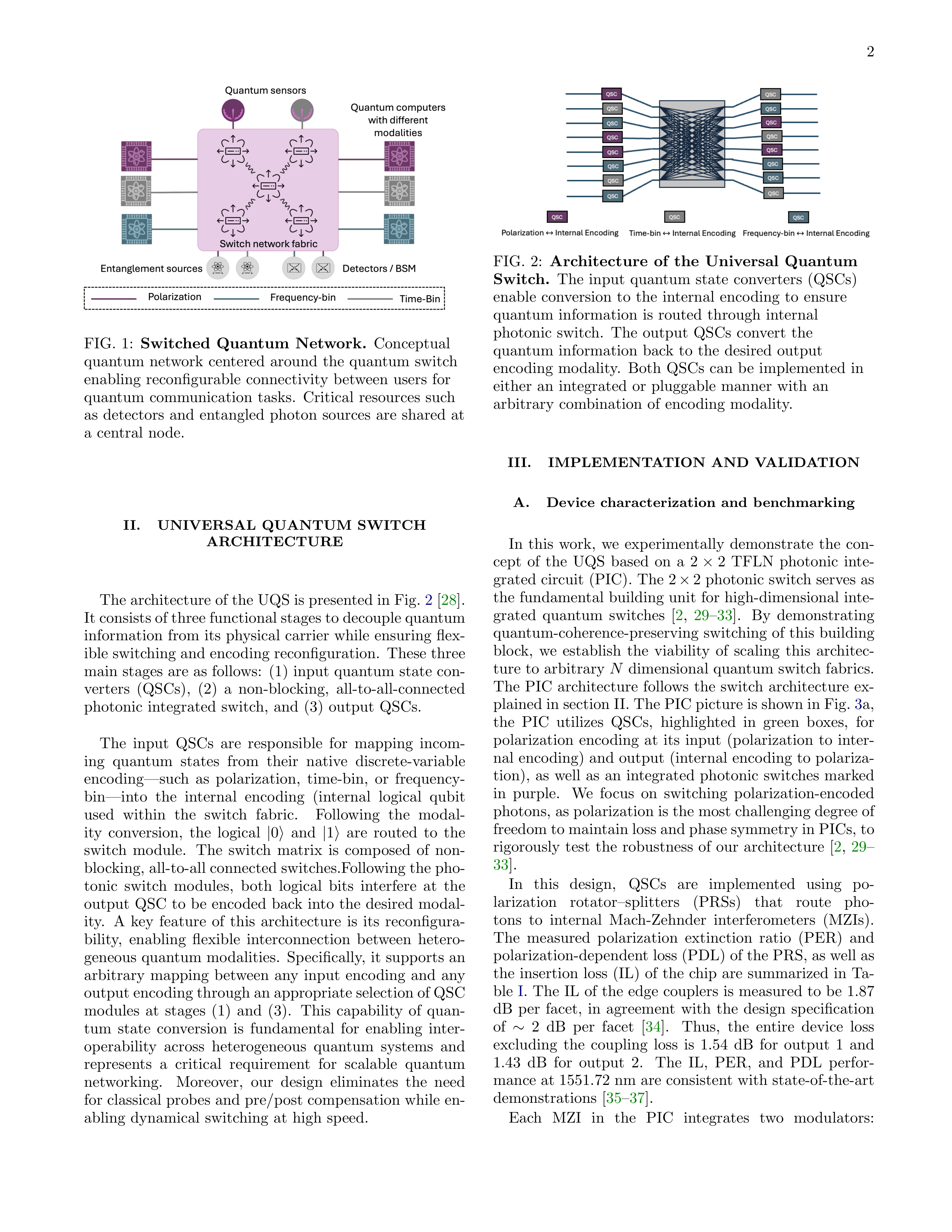
Fig.
1
).
The
pro-
posed
UQS
enables
on-demand,
non-blocking,
encoding-
agnostic switching of quantum information while preserv-
ing
quantum
coherence.
This
allows
seamless
interoper-
ability between heterogeneous quantum devices and facil-
itates
efficient
resource
sharing
[
27
].
By
overcoming
the
limitations
of
conventional
optical
switches
and
enabling
dynamic
quantum
state
distribution,
the
UQS
provides
the
essential
functionality
required
for
scalable
quan-
tum
network
architectures,
including
distributed
quan-
tum
computing
and
entanglement-as-a-service.
The
remainder
of
the
paper
is
organized
as
follows.
We
first
introduce
the
concept
and
architecture
of
the
Universal
Quantum
Switch
in
Section
II
.
After
this,
we
show
a
proof-of-concept
demonstration
of
our
archi-
tecture
based
on
a
thin-film
lithium
niobate
(TFLN)
switch
specifically
designed
for
polarization
encoding.
Section
III A
presents
the
device
benchmarking
results,
including
classical
and
quantum
characterizations.
In
Section
III B
,
we
demonstrate
entanglement-preserving
switching
for
an
arbitrary
entangled
state
under
both
thermo-
and
electro-optic
modulation.
Finally,
the
scal-
ing potential of our architecture is analyzed in Section
IV
.
2
FIG.
1:
Switched
Quantum
Network.
Conceptual
quantum
network
centered
around
the
quantum
switch
enabling
reconfigurable
connectivity
between
users
for
quantum
communication
tasks.
Critical
resources
such
as
detectors
and
entangled
photon
sources
are
shared
at
a
central
node.
II.
UNIVERSAL
QUANTUM
SWITCH
ARCHITECTURE
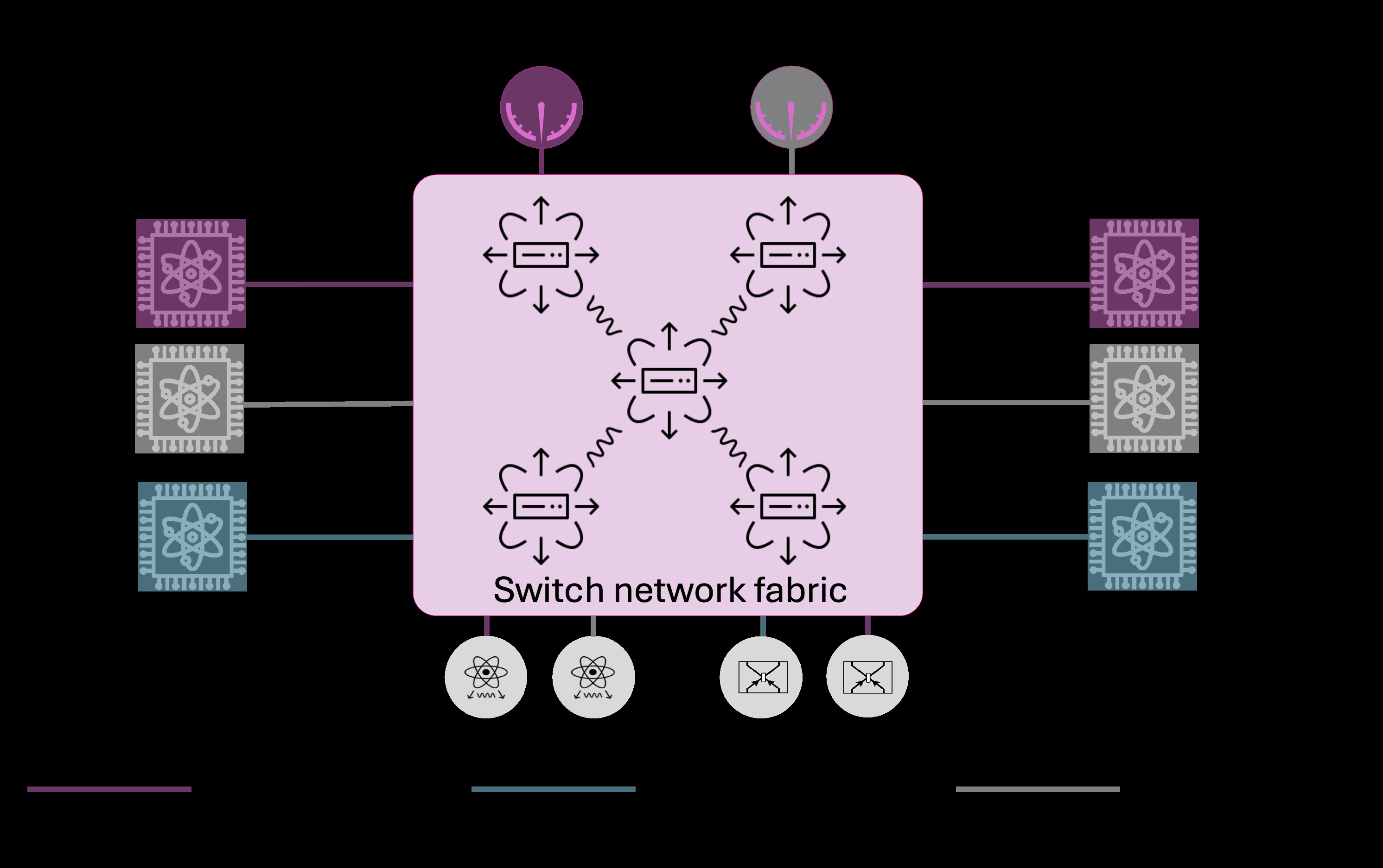
The architecture of the UQS is presented in Fig.
2
[
28
].
It consists of three functional stages to decouple quantum
information
from
its
physical
carrier
while
ensuring
flex-
ible switching and encoding reconfiguration.
These three
main
stages
are
as
follows:
(1)
input
quantum
state
con-
verters
(QSCs),
(2)
a
non-blocking,
all-to-all-connected
photonic
integrated
switch,
and
(3)
output
QSCs.
The
input
QSCs
are
responsible
for
mapping
incom-
ing
quantum
states
from
their
native
discrete-variable
encoding—such
as
polarization,
time-bin,
or
frequency-
bin—into
the
internal
encoding
(internal
logical
qubit
used
within
the
switch
fabric.
Following
the
modal-
ity
conversion,
the
logical
|
0
⟩
and
|
1
⟩
are
routed
to
the
switch
module.
The
switch
matrix
is
composed
of
non-
blocking, all-to-all connected switches.Following the pho-
tonic
switch
modules,
both
logical
bits
interfere
at
the
output
QSC
to
be
encoded
back
into
the
desired
modal-
ity.
A
key
feature
of
this
architecture
is
its
reconfigura-
bility,
enabling
flexible
interconnection
between
hetero-
geneous
quantum
modalities.
Specifically,
it
supports
an
arbitrary
mapping
between
any
input
encoding
and
any
output encoding through an appropriate selection of QSC
modules
at
stages
(1)
and
(3).
This
capability
of
quan-
tum
state
conversion
is
fundamental
for
enabling
inter-
operability
across
heterogeneous
quantum
systems
and
represents
a
critical
requirement
for
scalable
quantum
networking.
Moreover,
our
design
eliminates
the
need
for classical probes and pre/post compensation while en-
abling
dynamical
switching
at
high
speed.
FIG.
2:
Architecture
of
the
Universal
Quantum
Switch.
The
input
quantum
state
converters
(QSCs)
enable
conversion
to
the
internal
encoding
to
ensure
quantum
information
is
routed
through
internal
photonic
switch.
The
output
QSCs
convert
the
quantum
information
back
to
the
desired
output
encoding
modality.
Both
QSCs
can
be
implemented
in
either
an
integrated
or
pluggable
manner
with
an
arbitrary
combination
of
encoding
modality.
III.
IMPLEMENTATION
AND
VALIDATION
A.
Device
characterization
and
benchmarking
In
this
work,
we
experimentally
demonstrate
the
con-
cept
of
the
UQS
based
on
a
2
×
2
TFLN
photonic
inte-
grated
circuit
(PIC).
The
2
×
2
photonic
switch
serves
as
the
fundamental
building
unit
for
high-dimensional
inte-
grated
quantum
switches
[
2
,
29
–
33
].
By
demonstrating
quantum-coherence-preserving
switching
of
this
building
block,
we
establish
the
viability
of
scaling
this
architec-
ture
to
arbitrary
N
dimensional
quantum
switch
fabrics.
The
PIC
architecture
follows
the
switch
architecture
ex-
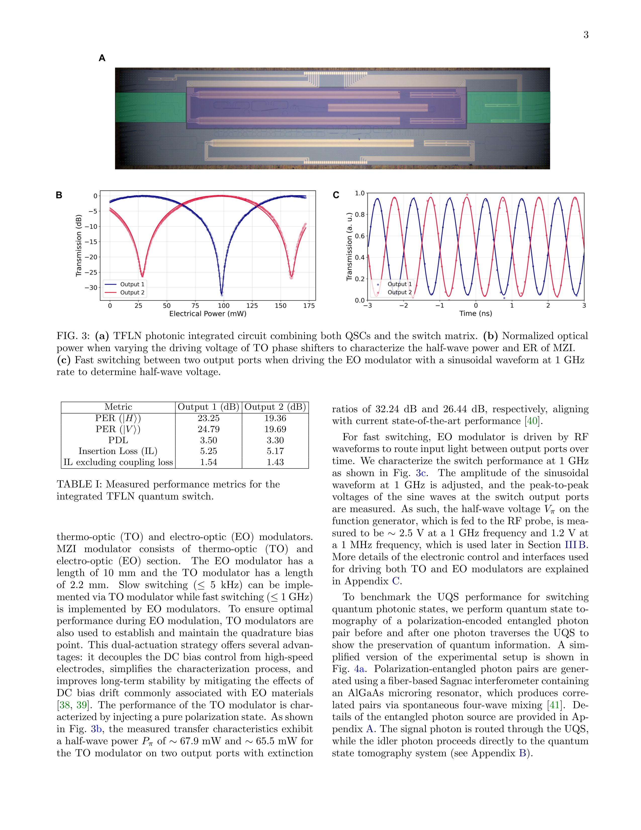
plained in section II. The PIC picture is shown in Fig.
3
a,
the
PIC
utilizes
QSCs,
highlighted
in
green
boxes,
for
polarization
encoding
at
its
input
(polarization
to
inter-
nal
encoding)
and
output
(internal
encoding
to
polariza-
tion),
as
well
as
an
integrated
photonic
switches
marked
in
purple.
We
focus
on
switching
polarization-encoded
photons, as polarization is the most challenging degree of
freedom to maintain loss and phase symmetry in PICs, to
rigorously
test
the
robustness
of
our
architecture
[
2
,
29
–
33
].
In
this
design,
QSCs
are
implemented
using
po-
larization
rotator–splitters
(PRSs)
that
route
pho-
tons
to
internal
Mach-Zehnder
interferometers
(MZIs).
The
measured
polarization
extinction
ratio
(PER)
and
polarization-dependent loss (PDL) of the PRS, as well as
the
insertion
loss
(IL)
of
the
chip
are
summarized
in
Ta-
ble
I
.
The
IL
of
the
edge
couplers
is
measured
to
be
1.87
dB
per
facet,
in
agreement
with
the
design
specification
of
∼
2
dB
per
facet
[
34
].
Thus,
the
entire
device
loss
excluding
the
coupling
loss
is
1.54
dB
for
output
1
and
1.43
dB
for
output
2.
The
IL,
PER,
and
PDL
perfor-
mance at 1551.72 nm are consistent with state-of-the-art
demonstrations
[
35
–
37
].
Each
MZI
in
the
PIC
integrates
two
modulators:
3
FIG.
3:
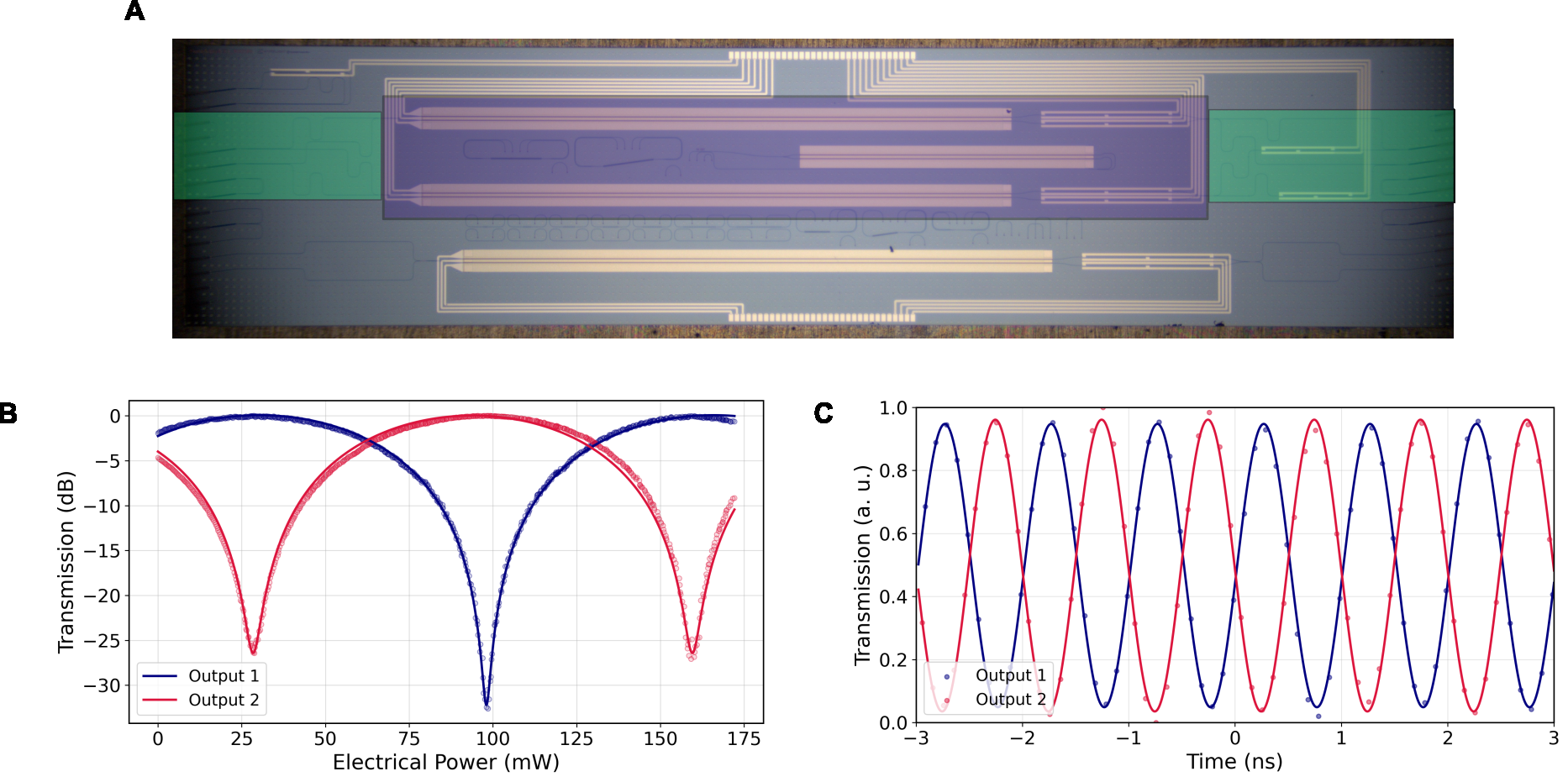
(a)
TFLN
photonic
integrated
circuit
combining
both
QSCs
and
the
switch
matrix.
(b)
Normalized
optical
power
when
varying
the
driving
voltage
of
TO
phase
shifters
to
characterize
the
half-wave
power
and
ER
of
MZI.
(c)
Fast
switching
between
two
output
ports
when
driving
the
EO
modulator
with
a
sinusoidal
waveform
at
1
GHz
rate
to
determine
half-wave
voltage.
Metric
Output
1
(dB)
Output
2
(dB)
PER
(
|
H
⟩
)
23.25
19.36
PER
(
|
V
⟩
)
24.79
19.69
PDL
3.50
3.30
Insertion
Loss
(IL)
5.25
5.17
IL
excluding
coupling
loss
1.54
1.43
TABLE
I:
Measured
performance
metrics
for
the
integrated
TFLN
quantum
switch.
thermo-optic
(TO)
and
electro-optic
(EO)
modulators.
MZI
modulator
consists
of
thermo-optic
(TO)
and
electro-optic
(EO)
section.
The
EO
modulator
has
a
length
of
10
mm
and
the
TO
modulator
has
a
length
of
2
.
2
mm.
Slow
switching
(
≤
5
kHz)
can
be
imple-
mented via TO modulator while fast switching (
≤
1 GHz)
is
implemented
by
EO
modulators.
To
ensure
optimal
performance
during
EO
modulation,
TO
modulators
are
also
used
to
establish
and
maintain
the
quadrature
bias
point.
This
dual-actuation
strategy
offers
several
advan-
tages:
it
decouples
the
DC
bias
control
from
high-speed
electrodes,
simplifies
the
characterization
process,
and
improves
long-term
stability
by
mitigating
the
effects
of
DC
bias
drift
commonly
associated
with
EO
materials
[
38
,
39
].
The
performance
of
the
TO
modulator
is
char-
acterized by injecting a pure polarization state.
As shown
in
Fig.
3
b
,
the
measured
transfer
characteristics
exhibit
a
half-wave
power
P
π
of
∼
67
.
9
mW
and
∼
65
.
5
mW
for
the
TO
modulator
on
two
output
ports
with
extinction
ratios
of
32.24
dB
and
26.44
dB,
respectively,
aligning
with
current
state-of-the-art
performance
[
40
].
For
fast
switching,
EO
modulator
is
driven
by
RF
waveforms to route input light between output ports over
time.
We
characterize
the
switch
performance
at
1
GHz
as
shown
in
Fig.
3
c
.
The
amplitude
of
the
sinusoidal
waveform
at
1
GHz
is
adjusted,
and
the
peak-to-peak
voltages
of
the
sine
waves
at
the
switch
output
ports
are
measured.
As
such,
the
half-wave
voltage
V
π
on
the
function generator, which is fed to the RF probe, is mea-
sured
to
be
∼
2.5
V
at
a
1
GHz
frequency
and
1.2
V
at
a
1
MHz
frequency,
which
is
used
later
in
Section
III B
.
More
details
of
the
electronic
control
and
interfaces
used
for
driving
both
TO
and
EO
modulators
are
explained
in
Appendix
C
.
To
benchmark
the
UQS
performance
for
switching
quantum
photonic
states,
we
perform
quantum
state
to-
mography
of
a
polarization-encoded
entangled
photon
pair
before
and
after
one
photon
traverses
the
UQS
to
show
the
preservation
of
quantum
information.
A
sim-
plified
version
of
the
experimental
setup
is
shown
in
Fig.
4
a
.
Polarization-entangled
photon
pairs
are
gener-
ated using a fiber-based Sagnac interferometer containing
an
AlGaAs
microring
resonator,
which
produces
corre-
lated
pairs
via
spontaneous
four-wave
mixing
[
41
].
De-
tails
of
the
entangled
photon
source
are
provided
in
Ap-
pendix
A
. The signal photon is routed through the UQS,
while
the
idler
photon
proceeds
directly
to
the
quantum
state
tomography
system
(see
Appendix
B
).
4
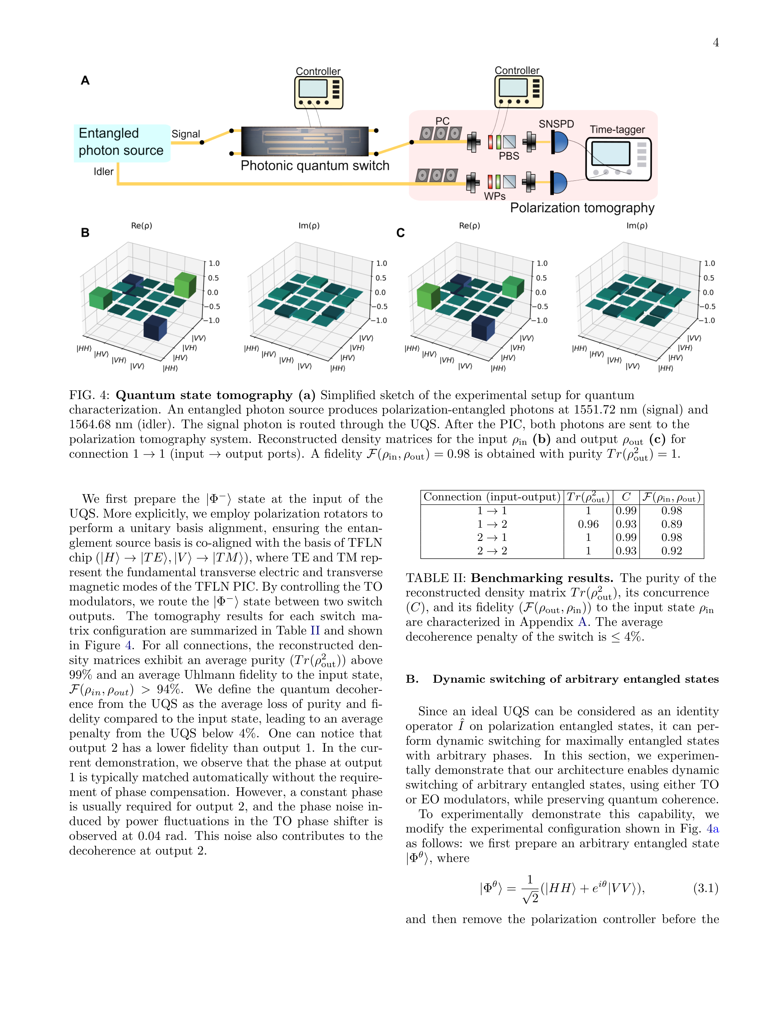
FIG.
4:
Quantum
state
tomography
(a)
Simplified
sketch
of
the
experimental
setup
for
quantum
characterization.
An
entangled
photon
source
produces
polarization-entangled
photons
at
1551
.
72
nm
(signal)
and
1564
.
68
nm
(idler).
The
signal
photon
is
routed
through
the
UQS.
After
the
PIC,
both
photons
are
sent
to
the
polarization
tomography
system.
Reconstructed
density
matrices
for
the
input
ρ
in
(b)
and
output
ρ
out
(c)
for
connection
1
→
1
(input
→
output
ports).
A
fidelity
F
(
ρ
in
, ρ
out
) = 0
.
98
is
obtained
with
purity
Tr
(
ρ
2
out
) = 1.
We
first
prepare
the
|
Φ
−
⟩
state
at
the
input
of
the
UQS. More explicitly, we employ polarization rotators to
perform
a
unitary
basis
alignment,
ensuring
the
entan-
glement source basis is co-aligned with the basis of TFLN
chip (
|
H
⟩→|
TE
⟩
,
|
V
⟩→|
TM
⟩
), where TE and TM rep-
resent the fundamental transverse electric and transverse
magnetic modes of the TFLN PIC. By controlling the TO
modulators,
we
route
the
|
Φ
−
⟩
state
between
two
switch
outputs.
The
tomography
results
for
each
switch
ma-
trix
configuration
are
summarized
in
Table
II
and
shown
in
Figure
4
.
For
all
connections,
the
reconstructed
den-
sity
matrices
exhibit
an
average
purity
(
Tr
(
ρ
2
out
))
above
99%
and
an
average
Uhlmann
fidelity
to
the
input
state,
F
(
ρ
in
, ρ
out
)
>
94%.
We
define
the
quantum
decoher-
ence
from
the
UQS
as
the
average
loss
of
purity
and
fi-
delity compared to the input state, leading to an average
penalty
from
the
UQS
below
4%.
One
can
notice
that
output
2
has
a
lower
fidelity
than
output
1.
In
the
cur-
rent demonstration,
we
observe
that
the
phase
at output
1 is typically matched automatically without the require-
ment
of
phase
compensation.
However,
a
constant
phase
is
usually
required
for
output
2,
and
the
phase
noise
in-
duced
by
power
fluctuations
in
the
TO
phase
shifter
is
observed
at
0.04
rad.
This
noise
also
contributes
to
the
decoherence
at
output
2.
Connection
(input-output)
Tr
(
ρ
2
out
)
C
F
(
ρ
in
, ρ
out
)
1
→
1
1
0
.
99
0.98
1
→
2
0.96
0
.
93
0.89
2
→
1
1
0
.
99
0
.
98
2
→
2
1
0
.
93
0
.
92
TABLE
II:
Benchmarking
results.
The
purity
of
the
reconstructed
density
matrix
Tr
(
ρ
2
out
),
its
concurrence
(
C
),
and
its
fidelity
(
F
(
ρ
out
, ρ
in
))
to
the
input
state
ρ
in
are
characterized
in
Appendix
A
.
The
average
decoherence
penalty
of
the
switch
is
≤
4%.
B.
Dynamic
switching
of
arbitrary
entangled
states
Since
an
ideal
UQS
can
be
considered
as
an
identity
operator
ˆ
I
on
polarization
entangled
states,
it
can
per-
form
dynamic
switching
for
maximally
entangled
states
with
arbitrary
phases.
In
this
section,
we
experimen-
tally
demonstrate
that
our
architecture
enables
dynamic
switching
of
arbitrary
entangled
states,
using
either
TO
or
EO
modulators,
while
preserving
quantum
coherence.
To
experimentally
demonstrate
this
capability,
we
modify
the
experimental
configuration
shown
in
Fig.
4
a
as
follows:
we
first
prepare
an
arbitrary
entangled
state
|
Φ
θ
⟩
,
where
|
Φ
θ
⟩
=
1
√
2
(
|
HH
⟩
+
e
iθ
|
V V
⟩
)
,
(3.1)
and
then
remove
the
polarization
controller
before
the
5
UQS. After this modification, our system mimics a three-
node
entanglement
distribution
network
without
polar-
ization
tracking.
The
dynamic
switching
of
entangled
states
without
quantum
decoherence
in
such
a
system
has
not
been
demonstrated
yet,
which
we
characterize
below.
We
first
show
the
preservation
of
quantum
coher-
ence
under
TO
switching.
An
arbitrary
entangled
state
|
Φ
θ
=
−
0
.
49
π
⟩
is
prepared
and
sent
to
the
UQS.
By
con-
trolling
the
TO
modulators
for
logical
|
0
⟩
s
and
|
1
⟩
s,
the
quantum state is switched between output 1 and 2.
After
the UQS, photons are measured at the quantum state to-
mography
system
yielding
a
fidelity
of
96%
and
a
purity
above
99%
for
both
output
ports.
Next, we demonstrate the preservation of quantum co-
herence
under
EO
switching
at
1
MHz.
Another
entan-
gled
state
|
Φ
θ
=
−
0
.
58
π
⟩
is
prepared
to
show
the
flexibility
of our architecture.
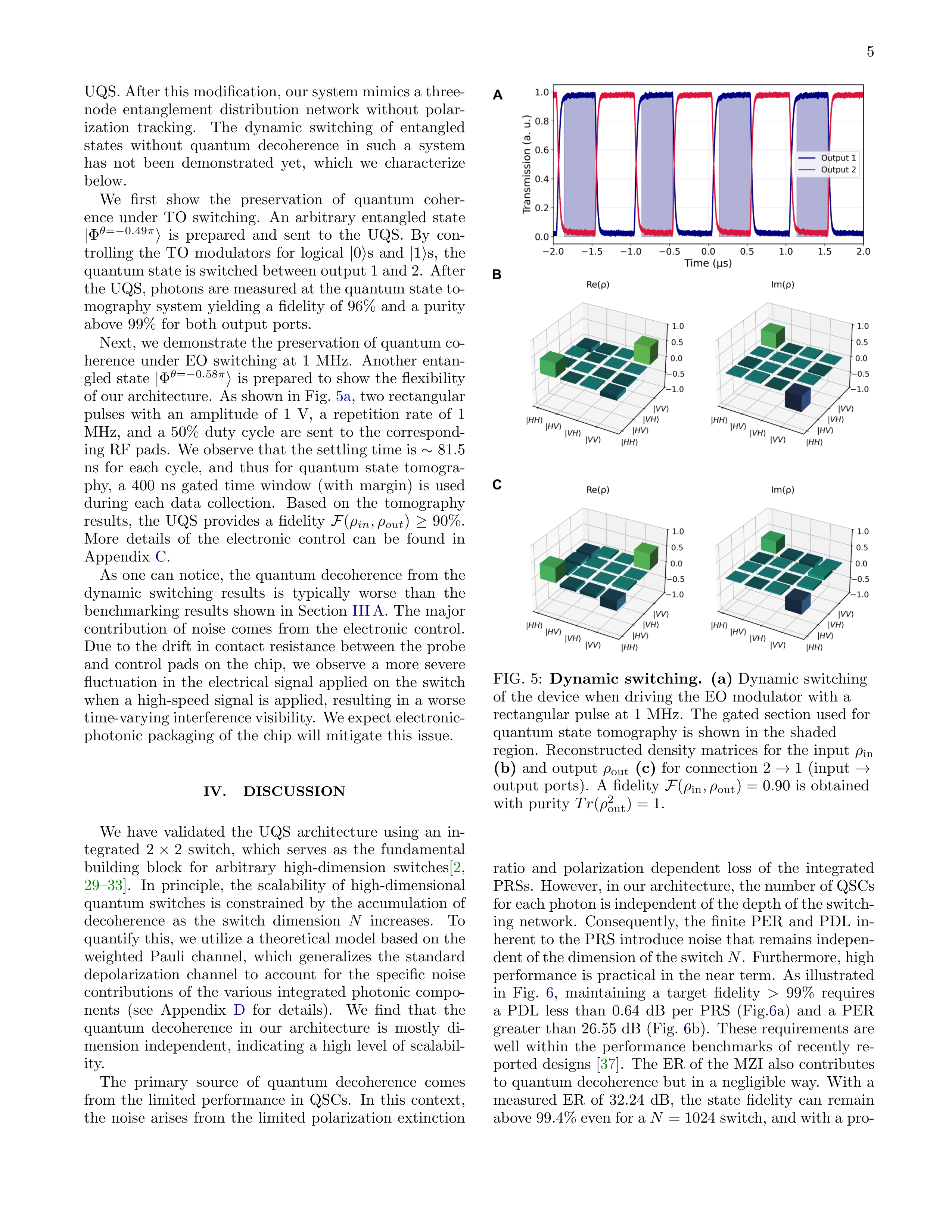
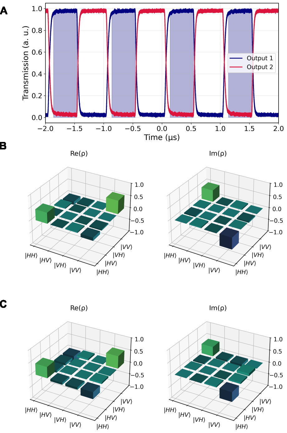
As shown in Fig.
5
a
, two rectangular
pulses
with
an
amplitude
of
1
V,
a
repetition
rate
of
1
MHz,
and
a
50%
duty
cycle
are
sent
to
the
correspond-
ing RF pads.
We observe that the settling time is
∼
81.5
ns
for
each
cycle,
and
thus
for
quantum
state
tomogra-
phy,
a
400
ns
gated
time
window
(with
margin)
is
used
during
each
data
collection.
Based
on
the
tomography
results,
the
UQS
provides
a
fidelity
F
(
ρ
in
, ρ
out
)
≥
90%.
More
details
of
the
electronic
control
can
be
found
in
Appendix
C
.
As
one
can
notice,
the
quantum
decoherence
from
the
dynamic
switching
results
is
typically
worse
than
the
benchmarking
results
shown
in
Section
III A
.
The
major
contribution
of
noise
comes
from
the
electronic
control.
Due
to
the
drift
in
contact
resistance
between
the
probe
and
control
pads
on
the
chip,
we
observe
a
more
severe
fluctuation
in
the
electrical
signal
applied
on
the
switch
when
a
high-speed
signal
is
applied,
resulting
in
a
worse
time-varying interference visibility.
We expect electronic-
photonic
packaging
of
the
chip
will
mitigate
this
issue.
IV.
DISCUSSION
We
have
validated
the
UQS
architecture
using
an
in-
tegrated
2
×
2
switch,
which
serves
as
the
fundamental
building
block
for
arbitrary
high-dimension
switches[
2
,
29
–
33
].
In
principle,
the
scalability
of
high-dimensional
quantum
switches
is
constrained
by
the
accumulation
of
decoherence
as
the
switch
dimension
N
increases.
To
quantify this, we utilize a theoretical model based on the
weighted
Pauli
channel,
which
generalizes
the
standard
depolarization
channel
to
account
for
the
specific
noise
contributions
of
the
various
integrated
photonic
compo-
nents
(see
Appendix
D
for
details).
We
find
that
the
quantum
decoherence
in
our
architecture
is
mostly
di-
mension
independent,
indicating
a
high
level
of
scalabil-
ity.
The
primary
source
of
quantum
decoherence
comes
from
the
limited
performance
in
QSCs.
In
this
context,
the
noise
arises
from
the
limited
polarization
extinction
FIG.
5:
Dynamic
switching.
(a)
Dynamic
switching
of
the
device
when
driving
the
EO
modulator
with
a
rectangular
pulse
at
1
MHz.
The
gated
section
used
for
quantum
state
tomography
is
shown
in
the
shaded
region.
Reconstructed
density
matrices
for
the
input
ρ
in
(b)
and
output
ρ
out
(c)
for
connection
2
→
1
(input
→
output
ports).
A
fidelity
F
(
ρ
in
, ρ
out
) = 0
.
90
is
obtained
with
purity
Tr
(
ρ
2
out
) = 1.
ratio
and
polarization
dependent
loss
of
the
integrated
PRSs.
However, in our architecture, the number of QSCs
for each photon is independent of the depth of the switch-
ing
network.
Consequently,
the
finite
PER
and
PDL
in-
herent to the PRS introduce noise that remains indepen-
dent of the dimension of the switch
N
.
Furthermore, high
performance
is
practical
in
the
near
term.
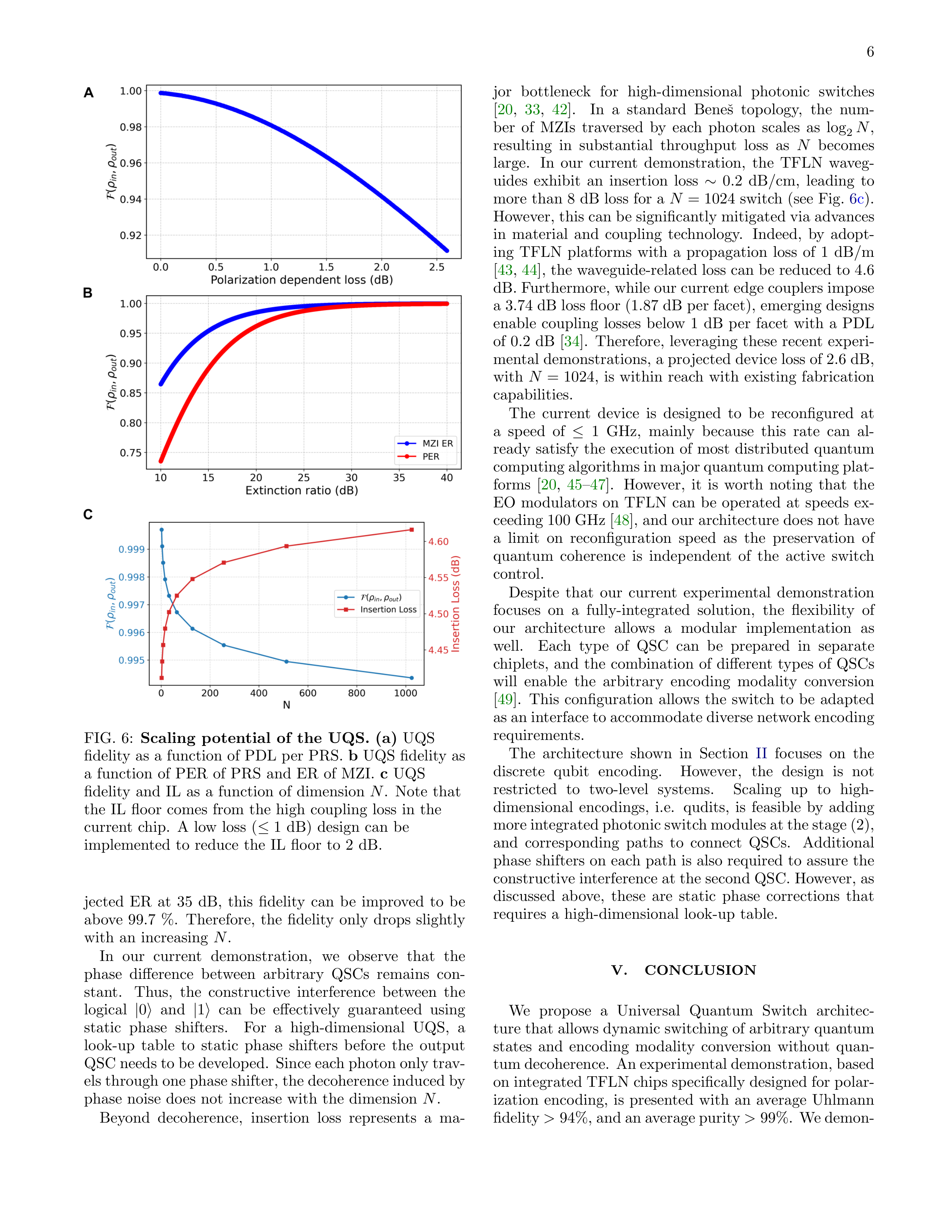
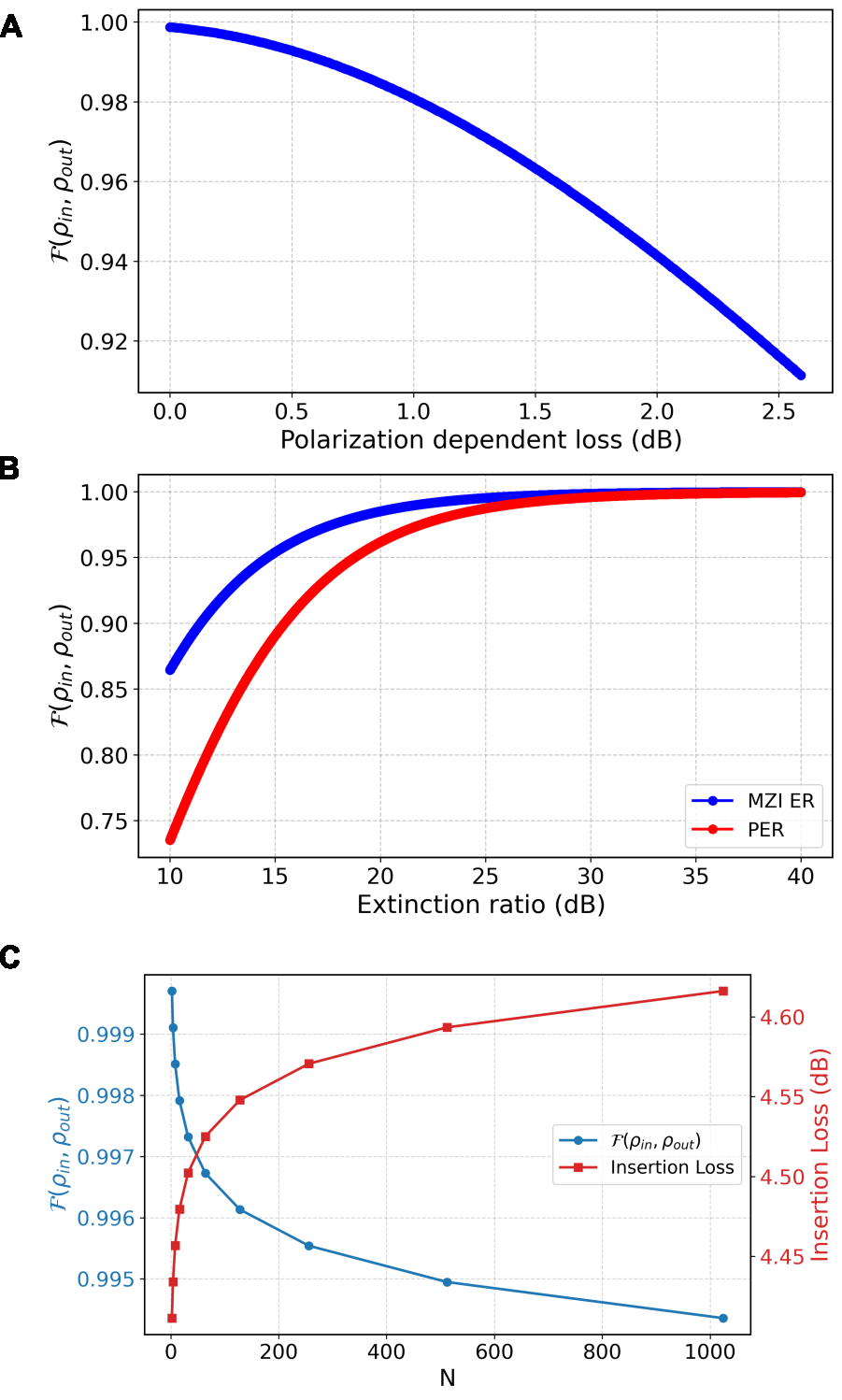
As
illustrated
in
Fig.
6
,
maintaining
a
target
fidelity
>
99%
requires
a
PDL
less
than
0
.
64
dB
per
PRS
(Fig.
6
a)
and
a
PER
greater
than
26
.
55
dB
(Fig.
6
b).
These
requirements
are
well
within
the
performance
benchmarks
of
recently
re-
ported
designs
[
37
].
The
ER
of
the
MZI
also
contributes
to
quantum
decoherence
but
in
a
negligible
way.
With
a
measured
ER
of
32
.
24
dB,
the
state
fidelity
can
remain
above 99.4% even for a
N
= 1024 switch, and with a pro-
6
FIG.
6:
Scaling
potential
of
the
UQS.
(a)
UQS
fidelity
as
a
function
of
PDL
per
PRS.
b
UQS
fidelity
as
a
function
of
PER
of
PRS
and
ER
of
MZI.
c
UQS
fidelity
and
IL
as
a
function
of
dimension
N
.
Note
that
the
IL
floor
comes
from
the
high
coupling
loss
in
the
current
chip.
A
low
loss
(
≤
1
dB)
design
can
be
implemented
to
reduce
the
IL
floor
to
2
dB.
jected
ER
at
35
dB,
this
fidelity
can
be
improved
to
be
above
99.7
%.
Therefore,
the
fidelity
only
drops
slightly
with
an
increasing
N
.
In
our
current
demonstration,
we
observe
that
the
phase
difference
between
arbitrary
QSCs
remains
con-
stant.
Thus,
the
constructive
interference
between
the
logical
|
0
⟩
and
|
1
⟩
can
be
effectively
guaranteed
using
static
phase
shifters.
For
a
high-dimensional
UQS,
a
look-up
table
to
static
phase
shifters
before
the
output
QSC needs to be developed.
Since each photon only trav-
els through one phase shifter, the decoherence induced by
phase
noise
does
not
increase
with
the
dimension
N
.
Beyond
decoherence,
insertion
loss
represents
a
ma-
jor
bottleneck
for
high-dimensional
photonic
switches
[
20
,
33
,
42
].
In
a
standard
Beneˇs
topology,
the
num-
ber
of
MZIs
traversed
by
each
photon
scales
as
log
2
N
,
resulting
in
substantial
throughput
loss
as
N
becomes
large.
In
our
current
demonstration,
the
TFLN
waveg-
uides
exhibit
an
insertion
loss
∼
0.2
dB/cm,
leading
to
more
than
8
dB
loss
for
a
N
= 1024
switch
(see
Fig.
6
c
).
However, this can be significantly mitigated via advances
in
material
and
coupling
technology.
Indeed,
by
adopt-
ing
TFLN
platforms
with
a
propagation
loss
of
1
dB/m
[
43
,
44
],
the waveguide-related loss can be reduced to 4.6
dB. Furthermore, while our current edge couplers impose
a 3.74 dB loss floor (1.87 dB per facet), emerging designs
enable
coupling
losses
below
1
dB
per
facet
with
a
PDL
of
0.2
dB
[
34
].
Therefore,
leveraging
these
recent
experi-
mental demonstrations, a projected device loss of 2.6 dB,
with
N
= 1024,
is
within
reach
with
existing
fabrication
capabilities.
The
current
device
is
designed
to
be
reconfigured
at
a
speed
of
≤
1
GHz,
mainly
because
this
rate
can
al-
ready
satisfy
the
execution
of
most
distributed
quantum
computing algorithms in major quantum computing plat-
forms
[
20
,
45
–
47
].
However,
it
is
worth
noting
that
the
EO
modulators
on
TFLN
can
be
operated
at
speeds
ex-
ceeding 100 GHz [
48
], and our architecture does not have
a
limit
on
reconfiguration
speed
as
the
preservation
of
quantum
coherence
is
independent
of
the
active
switch
control.
Despite
that
our
current
experimental
demonstration
focuses
on
a
fully-integrated
solution,
the
flexibility
of
our
architecture
allows
a
modular
implementation
as
well.
Each
type
of
QSC
can
be
prepared
in
separate
chiplets,
and
the
combination
of
different
types
of
QSCs
will
enable
the
arbitrary
encoding
modality
conversion
[
49
].
This
configuration
allows
the
switch
to
be
adapted
as an interface to accommodate diverse network encoding
requirements.
The
architecture
shown
in
Section
II
focuses
on
the
discrete
qubit
encoding.
However,
the
design
is
not
restricted
to
two-level
systems.
Scaling
up
to
high-
dimensional
encodings,
i.e.
qudits,
is
feasible
by
adding
more integrated photonic switch modules at the stage (2),
and
corresponding
paths
to
connect
QSCs.
Additional
phase
shifters
on
each
path
is
also
required
to
assure
the
constructive interference at the second QSC. However, as
discussed
above,
these
are
static
phase
corrections
that
requires
a
high-dimensional
look-up
table.
V.
CONCLUSION
We
propose
a
Universal
Quantum
Switch
architec-
ture that allows dynamic switching of arbitrary quantum
states
and
encoding
modality
conversion
without
quan-
tum decoherence.
An experimental demonstration, based
on integrated TFLN chips specifically designed for polar-
ization
encoding,
is
presented
with
an
average
Uhlmann
fidelity
>
94%, and an average purity
>
99%.
We demon-
7
strate robust switching of arbitrary entangled states with
a
quantum
decoherence
≤
4%
using
slow,
thermo-optic
operation,
and
≤
5%
using
fast,
electro-optic
operation.
To
the
best
of
our
knowledge,
the
UQS
is
the
first
ex-
perimental
demonstration
of
routing
arbitrary
entangled
states
at
MHz
rate
without
sacrificing
quantum
coher-
ence.
Based
on
the
theoretical
model
of
the
UQS,
our
architecture
only
introduces
additional
quantum
deco-
herence in a negligible amount with an increasing dimen-
sion
N
.
Therefore,
it
is
feasible
to
scale
up
the
UQS
at
a
minimal
decoherence
and
insertion
loss,
which
makes
the
UQS
a
fundamental
building
block
for
scalable
and
dynamically
reconfigurable
heterogeneous
quantum
net-
works.
VI.
ACKNOWLEDGEMENTS
The
authors
would
like
to
thank
Nathan
Liu,
Kevin
Luke and Marko Lonˇcar from Hyperlight Corporation for
helpful
discussions,
as
well
as
the
design
and
fabrication
of
the
TFLN
chips.
VII.
DATA
AVAILABILITY
The data sets used and analyzed in this study are avail-
able
from
the
corresponding
author
upon
reasonable
re-
quest.
Appendix
A:
Entangled
photon
source
A
detailed
schematic
of
the
entangled
photon
source
is
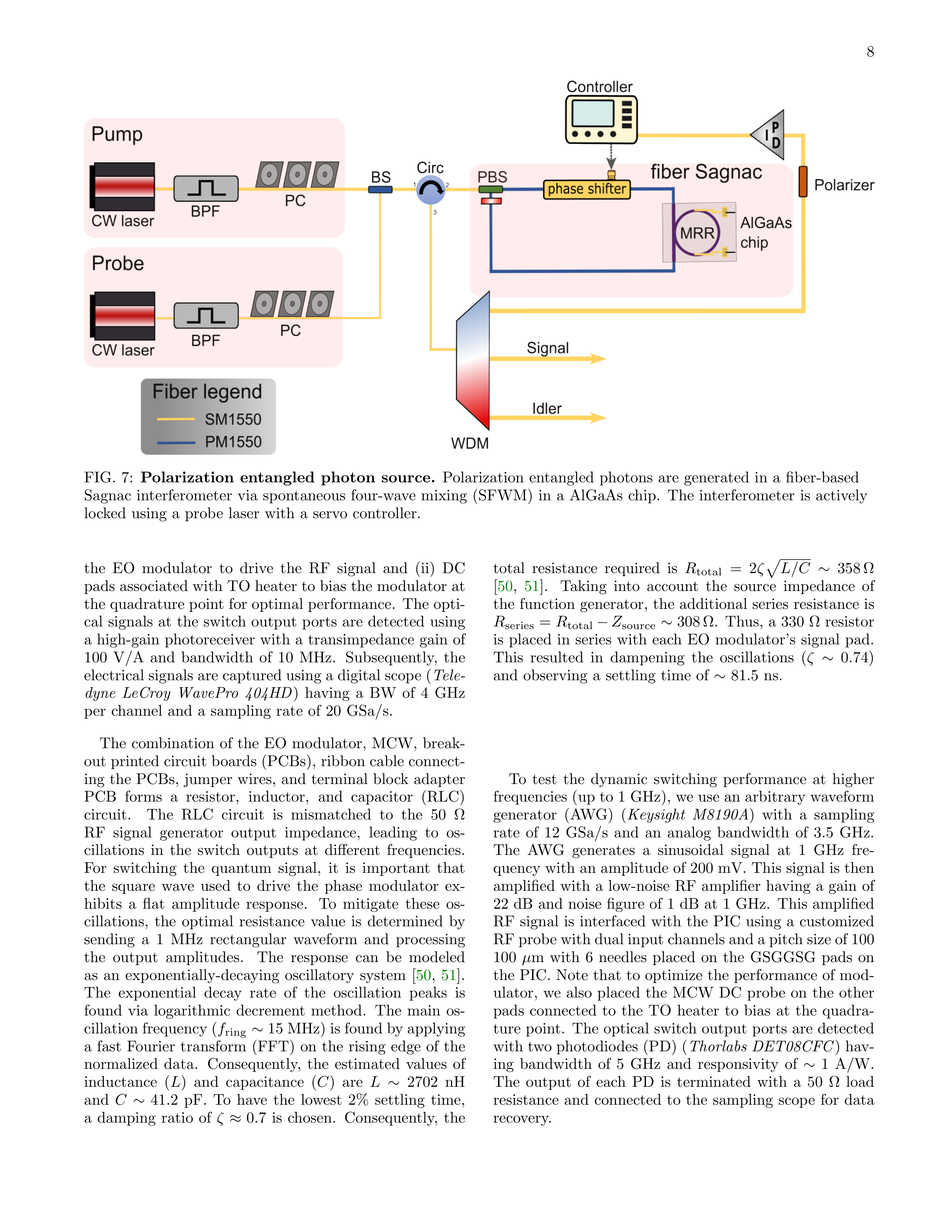
provided
in
Fig.
7
a
.
The
light
from
a
tunable
and
continuous
wave
laser
(
Keysight
N7778C
)
is
coupled
to
a
fiber-based
Sagnac
interferometer.
A
polarization
con-
troller
at
the
input
of
the
Sagnac
loop
sets
the
pump
polarization
to
the
anti-diagonal
polarization
state
|
A
⟩
to
enable
bidirectional
excitation
of
the
resonator.
The
AlGaAs
micro-ring
resonator
has
a
loaded
Q
∼
2
×
10
5
with
a
free
spectral
range
of
400
GHz.
The
counter-
propagating
pump
fields
generate
photon
pairs
in
in-
distinguishable
paths,
whose
superposition
results
in
polarization-entangled
states
at
the
interferometer
out-
put.
To
ensure
long-term
phase
stability
of
the
inter-
ferometer,
an
auxiliary
probe
laser
at
λ
aux
=
1542
.
14
nm
is
co-propagated
through
the
Sagnac
loop
and
used
for
active
phase
locking.
The
interference
signal
of
the
probe
is
monitored
and
fed
back
to
a
fiber
phase
shifter
driven
by
a
servo
controller
(
NewFocus
LB1005
),
al-
lowing
stabilization
of
the
relative
phase
between
the
counter-propagating paths.
The locking point can be ad-
justed
to
control
the
phase
of
the
entangled
state
|
Φ
θ
⟩
.
Following
the
Sagnac
loop,
the
signal
and
idler
photons
pass through an optical circulator and are then separated
using
an
ITU-grid
demultiplexer
(
Fiberdyne
Labs
).
The
source
system
exhibits
a
loss
of
23
.
7
and
22
.
7
dB
for
sig-
nal
and
idler
photons,
respectively.
These
losses
were
primarily
attributed
to
source
packaging
and
ITU
grid
demultiplexer.
Appendix
B:
Quantum
State
Tomography
To
reconstruct
the
density
matrix
of
entangled
states,
we
perform
quantum
state
tomography
on
the
entangled
photons
directly
emitted
from
the
source,
and
then
on
photons
after
the
UQS.
The
quantum
state
tomography
consists
of
motorized
polarization
analyzers,
each
comprising
free-space
colli-
mators, a quarter-wave plate, a half-wave plate, and a po-
larizing beam splitter, which are all broadband devices to
cover
the
entire
telecommunication
O
and
C
bands.
The
tomography
system
has
optical
losses
of
2
.
9
and
4
.
3
dB
for signal and idler photons,
respectively.
After the colli-
mators, both photons are detected with superconducting
nanowire
single-photon
detectors
(SNSPDs),
and
coinci-
dence
events
are
registered
using
a
time-tagger
(
Swabian
instruments
Time
Tagger
X
).
The
SNSPD
(
ID
Quan-
tique
)
has
a
quantum
efficiency
of
≥
85%
and
a
timing
resolution
of
≤
30
ps.
Using
a
standard
maximum
likelihood
estimation,
we
reconstruct the density matrix based on correlation mea-
surement
results.
As
shown
in
Fig.
4
b
,
the
density
ma-
trix
of
the
source,
ρ
in
,
is
reconstructed.
We
obtain
an
Uhlmann
fidelity
F
(
ρ
in
,
|
Φ
−
⟩⟨
Φ
−
|
)
=
0
.
97
to
the
|
Φ
−
⟩
Bell
state,
with
purity
Tr(
ρ
2
in
)
=
1
and
concurrence
C
= 0
.
99.
Appendix
C:
Electronic
interfaces
To characterize the TO modulation, the corresponding
DC pads connected to the phase shifters are driven using
a
multi-contact
wedge
(MCW)
probe
with
32
Tungsten
needles
at
100
µ
m
pitch.
We
note
that
the
measured
re-
sistance of the phase shifters placed in the TO modulator
is
∼
600Ωand that of the ones placed in the output QSCs
is
∼
300Ω, which matches the design specifications.These
values match the design specifications since the length of
the
phase
shifter
in
the
TO
modulator
is
twice
that
of
the other.
All measurements with the DC probe are per-
formed
under
constant
current
operation.
We
observe
a
fluctuation
in
the
measured
contact
resistance,
leading
to
phase
noises
on
the
TO
phase
shifters
as
reported
in
Sec.
III A
.
To
explain
the
hardware
devices
used
to
drive
the
TO
or EO modulators in detail, we divide the electronic con-
trol
system
into
two
operation
regimes.
To
test
dynamic
switching
at
frequencies
<
50
MHz,
a
function
gener-
ator
(
Keysight
33622A
)
is
used
to
generate
two
phase-
synchronized
square
waves.
The
function
generator
in-
terfaces with the PIC using a DC probe.
Thus, the MCW
is placed on both (i) ground-state-ground (GSG) pads of
8
FIG.
7:
Polarization
entangled
photon
source.
Polarization
entangled
photons
are
generated
in
a
fiber-based
Sagnac
interferometer
via
spontaneous
four-wave
mixing
(SFWM)
in
a
AlGaAs
chip.
The
interferometer
is
actively
locked
using
a
probe
laser
with
a
servo
controller.
the
EO
modulator
to
drive
the
RF
signal
and
(ii)
DC
pads associated with TO heater to bias the modulator at
the quadrature point for optimal performance.
The opti-
cal
signals
at
the
switch
output
ports
are
detected
using
a
high-gain
photoreceiver
with
a
transimpedance
gain
of
100
V/A
and
bandwidth
of
10
MHz.
Subsequently,
the
electrical signals are captured using a digital scope (
Tele-
dyne
LeCroy
WavePro
404HD
)
having
a
BW
of
4
GHz
per
channel
and
a
sampling
rate
of
20
GSa/s.
The
combination
of
the
EO
modulator,
MCW,
break-
out printed circuit boards (PCBs), ribbon cable connect-
ing
the
PCBs,
jumper
wires,
and
terminal
block
adapter
PCB
forms
a
resistor,
inductor,
and
capacitor
(RLC)
circuit.
The
RLC
circuit
is
mismatched
to
the
50
Ω
RF
signal
generator
output
impedance,
leading
to
os-
cillations
in
the
switch
outputs
at
different
frequencies.
For
switching
the
quantum
signal,
it
is
important
that
the
square
wave
used
to
drive
the
phase
modulator
ex-
hibits
a
flat
amplitude
response.
To
mitigate
these
os-
cillations,
the
optimal
resistance
value
is
determined
by
sending
a
1
MHz
rectangular
waveform
and
processing
the
output
amplitudes.
The
response
can
be
modeled
as
an
exponentially-decaying
oscillatory
system
[
50
,
51
].
The
exponential
decay
rate
of
the
oscillation
peaks
is
found
via
logarithmic
decrement
method.
The
main
os-
cillation frequency (
f
ring
∼
15 MHz) is found by applying
a
fast
Fourier
transform
(FFT)
on
the
rising
edge
of
the
normalized
data.
Consequently,
the
estimated
values
of
inductance
(
L
)
and
capacitance
(
C
)
are
L
∼
2702
nH
and
C
∼
41
.
2
pF.
To
have
the
lowest
2%
settling
time,
a
damping
ratio
of
ζ
≈
0
.
7
is
chosen.
Consequently,
the
total
resistance
required
is
R
total
=
2
ζ
p
L/C
∼
358 Ω
[
50
,
51
].
Taking
into
account
the
source
impedance
of
the
function
generator,
the
additional
series
resistance
is
R
series
=
R
total
−
Z
source
∼
308 Ω.
Thus,
a
330
Ωresistor
is
placed
in
series
with
each
EO
modulator’s
signal
pad.
This
resulted
in
dampening
the
oscillations
(
ζ
∼
0
.
74)
and
observing
a
settling
time
of
∼
81.5
ns.
To
test
the
dynamic
switching
performance
at
higher
frequencies (up to 1 GHz), we use an arbitrary waveform
generator
(AWG)
(
Keysight
M8190A
)
with
a
sampling
rate
of
12
GSa/s
and
an
analog
bandwidth
of
3.5
GHz.
The
AWG
generates
a
sinusoidal
signal
at
1
GHz
fre-
quency with an amplitude of 200 mV. This signal is then
amplified
with
a
low-noise
RF
amplifier
having
a
gain
of
22
dB
and
noise
figure
of
1
dB
at
1
GHz.
This
amplified
RF
signal
is
interfaced
with
the
PIC
using
a
customized
RF probe with dual input channels and a pitch size of 100
100
µ
m
with
6
needles
placed
on
the
GSGGSG
pads
on
the
PIC.
Note
that
to
optimize
the
performance
of
mod-
ulator,
we
also
placed
the
MCW
DC
probe
on
the
other
pads
connected
to
the
TO
heater
to
bias
at
the
quadra-
ture
point.
The
optical
switch
output
ports
are
detected
with two photodiodes (PD) (
Thorlabs
DET08CFC
) hav-
ing
bandwidth
of
5
GHz
and
responsivity
of
∼
1
A/W.
The
output
of
each
PD
is
terminated
with
a
50
Ωload
resistance
and
connected
to
the
sampling
scope
for
data
recovery.
9
Appendix
D:
Theoretical
model
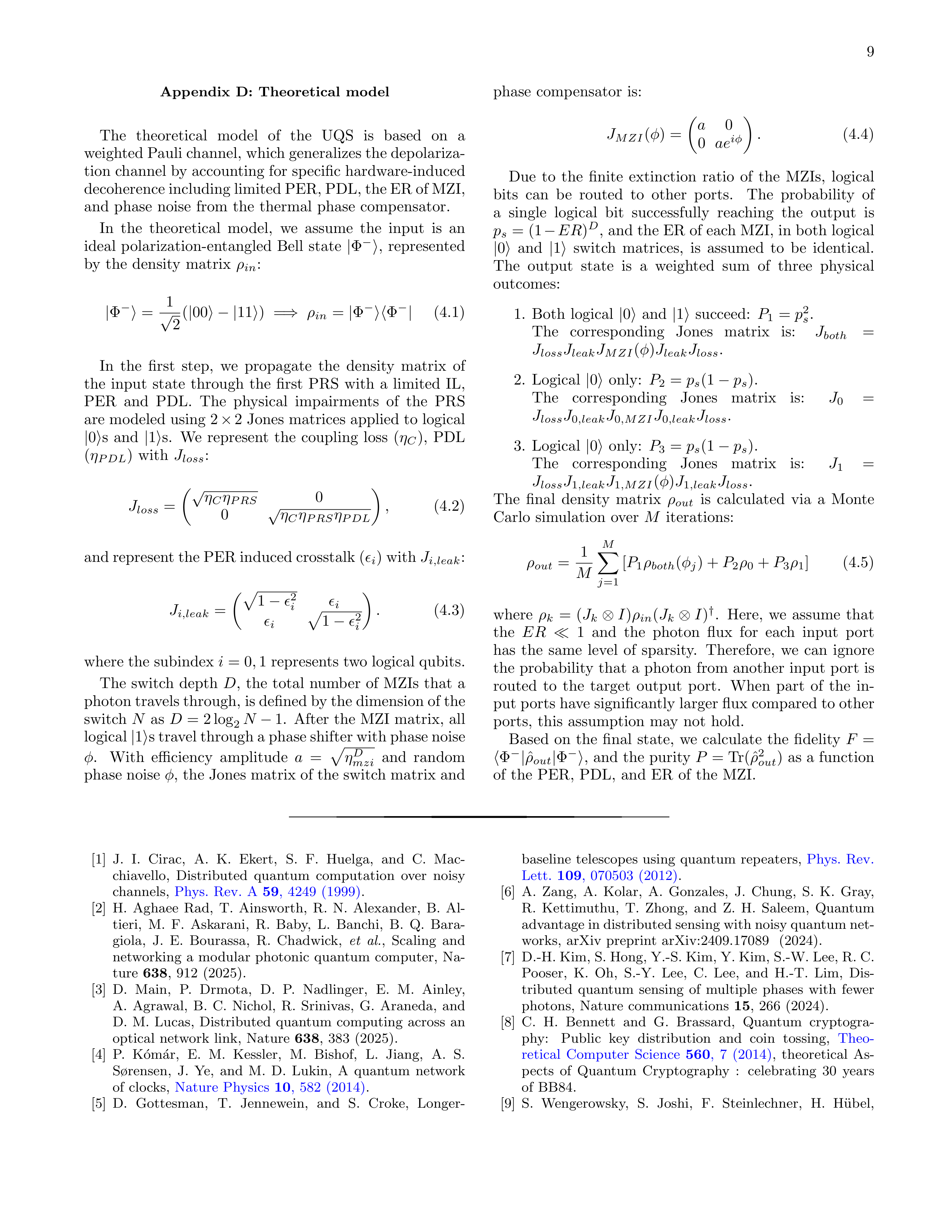
The
theoretical
model
of
the
UQS
is
based
on
a
weighted Pauli channel, which generalizes the depolariza-
tion channel by accounting for specific hardware-induced
decoherence including limited PER, PDL, the ER of MZI,
and
phase
noise
from
the
thermal
phase
compensator.
In
the
theoretical
model,
we
assume
the
input
is
an
ideal
polarization-entangled
Bell
state
|
Φ
−
⟩
,
represented
by
the
density
matrix
ρ
in
:
|
Φ
−
⟩
=
1
√
2
(
|
00
⟩−|
11
⟩
)
=
⇒
ρ
in
=
|
Φ
−
⟩⟨
Φ
−
|
(4.1)
In
the
first
step,
we
propagate
the
density
matrix
of
the
input
state
through
the
first
PRS
with
a
limited
IL,
PER
and
PDL.
The
physical
impairments
of
the
PRS
are modeled using 2
×
2 Jones matrices applied to logical
|
0
⟩
s
and
|
1
⟩
s.
We
represent
the
coupling
loss
(
η
C
),
PDL
(
η
P DL
)
with
J
loss
:
J
loss
=
√
η
C
η
P RS
0
0
√
η
C
η
P RS
η
P DL
,
(4.2)
and represent the PER induced crosstalk (
ϵ
i
) with
J
i,leak
:
J
i,leak
=
p
1
−
ϵ
2
i
ϵ
i
ϵ
i
p
1
−
ϵ
2
i
.
(4.3)
where the subindex
i
= 0
,
1 represents two logical qubits.
The
switch
depth
D
,
the
total
number
of
MZIs
that
a
photon travels through, is defined by the dimension of the
switch
N
as
D
= 2 log
2
N
−
1.
After
the
MZI
matrix,
all
logical
|
1
⟩
s travel through a phase shifter with phase noise
ϕ
.
With
efficiency
amplitude
a
=
p
η
D
mzi
and
random
phase noise
ϕ
, the Jones matrix of the switch matrix and
phase
compensator
is:
J
MZI
(
ϕ
) =
a
0
0
ae
iϕ
.
(4.4)
Due
to
the
finite
extinction
ratio
of
the
MZIs,
logical
bits
can
be
routed
to
other
ports.
The
probability
of
a
single
logical
bit
successfully
reaching
the
output
is
p
s
= (1
−
ER
)
D
, and the ER of each MZI, in both logical
|
0
⟩
and
|
1
⟩
switch
matrices,
is
assumed
to
be
identical.
The
output
state
is
a
weighted
sum
of
three
physical
outcomes:
1.
Both
logical
|
0
⟩
and
|
1
⟩
succeed:
P
1
=
p
2
s
.
The
corresponding
Jones
matrix
is:
J
both
=
J
loss
J
leak
J
MZI
(
ϕ
)
J
leak
J
loss
.
2.
Logical
|
0
⟩
only:
P
2
=
p
s
(1
−
p
s
).
The
corresponding
Jones
matrix
is:
J
0
=
J
loss
J
0
,leak
J
0
,MZI
J
0
,leak
J
loss
.
3.
Logical
|
0
⟩
only:
P
3
=
p
s
(1
−
p
s
).
The
corresponding
Jones
matrix
is:
J
1
=
J
loss
J
1
,leak
J
1
,MZI
(
ϕ
)
J
1
,leak
J
loss
.
The
final
density
matrix
ρ
out
is
calculated
via
a
Monte
Carlo
simulation
over
M
iterations:
ρ
out
=
1
M
M
X
j
=1
[
P
1
ρ
both
(
ϕ
j
) +
P
2
ρ
0
+
P
3
ρ
1
]
(4.5)
where
ρ
k
=
(
J
k
⊗
I
)
ρ
in
(
J
k
⊗
I
)
†
.
Here,
we
assume
that
the
ER
≪
1
and
the
photon
flux
for
each
input
port
has
the
same
level
of
sparsity.
Therefore,
we
can
ignore
the
probability
that
a
photon
from
another
input
port
is
routed
to
the
target
output
port.
When
part
of
the
in-
put ports have significantly larger flux compared to other
ports,
this
assumption
may
not
hold.
Based
on
the
final
state,
we
calculate
the
fidelity
F
=
⟨
Φ
−
|
ˆ
ρ
out
|
Φ
−
⟩
,
and
the
purity
P
= Tr(ˆ
ρ
2
out
)
as
a
function
of
the
PER,
PDL,
and
ER
of
the
MZI.
[1]
J.
I.
Cirac,
A.
K.
Ekert,
S.
F.
Huelga,
and
C.
Mac-
chiavello,
Distributed
quantum
computation
over
noisy
channels,
Phys.
Rev.
A
59
,
4249
(1999)
.
[2]
H.
Aghaee
Rad,
T.
Ainsworth,
R.
N.
Alexander,
B.
Al-
tieri,
M.
F.
Askarani,
R.
Baby,
L.
Banchi,
B.
Q.
Bara-
giola,
J.
E.
Bourassa,
R.
Chadwick,
et
al.
,
Scaling
and
networking
a
modular
photonic
quantum
computer,
Na-
ture
638
,
912
(2025).
[3]
D.
Main,
P.
Drmota,
D.
P.
Nadlinger,
E.
M.
Ainley,
A.
Agrawal,
B.
C.
Nichol,
R.
Srinivas,
G.
Araneda,
and
D.
M.
Lucas,
Distributed
quantum
computing
across
an
optical
network
link,
Nature
638
,
383
(2025).
[4]
P.
K´om´ar,
E.
M.
Kessler,
M.
Bishof,
L.
Jiang,
A.
S.
Sørensen,
J.
Ye,
and
M.
D.
Lukin,
A
quantum
network
of
clocks,
Nature
Physics
10
,
582
(2014)
.
[5]
D.
Gottesman,
T.
Jennewein,
and
S.
Croke,
Longer-
baseline
telescopes
using
quantum
repeaters,
Phys.
Rev.
Lett.
109
,
070503
(2012)
.
[6]
A.
Zang,
A.
Kolar,
A.
Gonzales,
J.
Chung,
S.
K.
Gray,
R.
Kettimuthu,
T.
Zhong,
and
Z.
H.
Saleem,
Quantum
advantage in distributed sensing with noisy quantum net-
works,
arXiv
preprint
arXiv:2409.17089
(2024).
[7]
D.-H. Kim, S. Hong, Y.-S. Kim, Y. Kim, S.-W. Lee, R. C.
Pooser,
K.
Oh,
S.-Y.
Lee,
C.
Lee,
and
H.-T.
Lim,
Dis-
tributed
quantum
sensing
of
multiple
phases
with
fewer
photons,
Nature
communications
15
,
266
(2024).
[8]
C.
H.
Bennett
and
G.
Brassard,
Quantum
cryptogra-
phy:
Public
key
distribution
and
coin
tossing,
Theo-
retical
Computer
Science
560
,
7
(2014)
,
theoretical
As-
pects
of
Quantum
Cryptography
:
celebrating
30
years
of
BB84.
[9]
S.
Wengerowsky,
S.
Joshi,
F.
Steinlechner,
H.
H¨ubel,
10
and
R.
Ursin,
An
entanglement-based
wavelength-
multiplexed
quantum
communication
network,
Nature
564
,
225
(2018)
.
[10]
S.
Joshi,
D.
Aktas,
S.
Wengerowsky,
M.
Lonˇcari´c,
S.
Neumann,
B.
Liu,
T.
Scheidl,
G.
Lorenzo,
Samec,
L.
Kling,
A.
Qiu,
M.
Razavi,
M.
Stipˇcevi´c,
J.
Rarity,
and
R.
Ursin,
A
trusted
node-free
eight-user
metropoli-
tan
quantum
communication
network,
Science
Advances
6
,
0959
(2020)
.
[11]
Y.-A.
Chen,
Q.
Zhang,
T.-Y.
Chen,
W.-Q.
Cai,
S.-K.
Liao,
J.
Zhang,
K.
Chen,
J.
Yin,
J.-G.
Ren,
Z.
Chen,
S.-L.
Han,
Q.
Yu,
K.
Liang,
F.
Zhou,
X.
Yuan,
M.-S.
Zhao, T.-Y. Wang, X. Jiang, L. Zhang, W.-Y. Liu, Y. Li,
Q. Shen, Y. Cao, C.-Y. Lu, R. Shu, J.-Y. Wang, L. Li, N.-
L.
Liu,
F.
Xu,
X.-B.
Wang,
C.-Z.
Peng,
and
J.-W.
Pan,
An
integrated
space-to-ground
quantum
communication
network
over
4,600
kilometres,
Nature
589
,
214
(2021)
.
[12]
T. Van Leent, M. Bock, F. Fertig, R. Garthoff, S. Eppelt,
Y.
Zhou,
P.
Malik,
M.
Seubert,
T.
Bauer,
W.
Rosenfeld,
et
al.
,
Entangling
single
atoms
over
33
km
telecom
fibre,
Nature
607
,
69
(2022).
[13]
Y.
Zhou,
P.
Malik,
F.
Fertig,
M.
Bock,
T.
Bauer,
T.
van
Leent,
W.
Zhang,
C.
Becher,
and
H.
Weinfurter,
Long-
lived
quantum
memory
enabling
atom-photon
entangle-
ment
over
101
km
of
telecom
fiber,
PRX
Quantum
5
,
020307
(2024).
[14]
A.
N.
Craddock,
T.
Cowan,
N.
Bigagli,
S.
Yekasiri,
D.
Robinson,
G.
B.
Portmann,
A.
Verma,
Z.
Guo,
M. Kilzer,
J. Zhao,
M. Flament,
J. Shabani,
R. Nejabati,
and
M.
Namazi,
High-rate
scalable
entanglement
swap-
ping
between
remote
entanglement
sources
on
deployed
new york city fibers
(2026),
arXiv:2602.15653 [quant-ph]
.
[15]
Y.
Zhang,
R.
Broberg,
A.
Zhu,
G.
Li,
L.
Ge,
J.
M.
Smith,
and
L.
Feng,
Classical-decisive
quantum
inter-
net
by
integrated
photonics,
Science
389
,
940
(2025)
,
https://www.science.org/doi/pdf/10.1126/science.adx6176
.
[16]
M.
Alshowkan,
B.
P.
Williams,
P.
G.
Evans,
N.
S.
Rao,
E.
M.
Simmerman,
H.-H.
Lu,
N.
B.
Lingaraju,
A.
M.
Weiner,
C.
E.
Marvinney,
Y.-Y.
Pai,
B.
J.
Lawrie,
N.
A.
Peters,
and
J.
M.
Lukens,
Reconfigurable
quantum
lo-
cal
area
network
over
deployed
fiber,
PRX
Quantum
2
,
040304
(2021)
.
[17]
S. Vinet, R. Tannous, and T. Jennewein, A reconfigurable
entanglement
distribution
network
suitable
for
connect-
ing multiple ground nodes with a satellite,
EPJ Quantum
Technology
12
,
8
(2025)
.
[18]
S.
Vinet,
D.
England,
C.-Q.
Xu,
and
T.
Jennewein,
Demonstration
of
a
reconfigurable
quantum
network
ar-
chitecture
suitable
for
ground-to-space
communication,
Optica
Quantum
4
,
14
(2026)
.
[19]
F.
Appas,
F.
Baboux,
M.
I.
Amanti,
A.
Lemaˆıtre,
F.
Boitier,
E.
Diamanti,
and
S.
Ducci,
Flexible
entanglement-distribution
network
with
an
AlGaAs
chip
for
secure
communications,
npj
Quantum
Information
7
,
118
(2021)
.
[20]
J. Zhao,
Y. Xu,
X. Lu,
E. Kaur,
M. Kilzer,
R. Kompella,
R. W. Boyd, and R. Nejabati, Scalable low-latency entan-
glement distribution for distributed quantum computing,
Optica
Quantum
3
,
606
(2025).
[21]
M.
A.
Hall,
J.
B.
Altepeter,
and
P.
Kumar,
Ultrafast
switching
of
photonic
entanglement,
Physical
review
let-
ters
106
,
053901
(2011).
[22]
P.
Wang,
S.
Baek,
M.
Yabuno,
S.
Miki,
H.
Terai,
and
F.
Kaneda,
Low-loss
polarization-maintaining
router
for
single
and
entangled
photons
at
a
telecom
wavelength,
Advanced
Quantum
Technologies
8
,
e00355
(2025).
[23]
M. Bornadel, S. Vinet, J. Zhao, A. Minoonfar, M. Kilzer,
R.
Kompella,
and
R.
Nejabati,
Towards
a
quantum
switch
preserving
polarization
entanglement,
in
Quan-
tum
Computing,
Communication,
and
Simulation
VI
,
Vol.
13919,
edited
by
P.
R.
Hemmer,
A.
L.
Migdall,
and
I. A. Burenkov, International Society for Optics and Pho-
tonics
(SPIE,
2026)
p.
139190F.
[24]
H.
J.
Kimble,
The
quantum
internet,
Nature
453
,
1023
(2008)
.
[25]
G.
Kurizki,
P.
Bertet,
Y.
Kubo,
K.
Mølmer,
D.
Pet-
rosyan,
P.
Rabl,
and
J.
Schmiedmayer,
Quantum
technologies
with
hybrid
systems,
Proceedings
of
the
National
Academy
of
Sciences
112
,
3866
(2015)
,
https://www.pnas.org/doi/pdf/10.1073/pnas.1419326112
.
[26]
V.
Nehra,
R.
J.
Birrittella,
C.
C.
Tison,
B.
K.
Malia,
Z.
S.
Smith,
D.
Heberle,
N.
J.
Barton,
A.
M.
Smith,
A. Brownell, M. L. Fanto,
et al.
, Photonic qubit encoding
interconversion
for
heterogeneous
quantum
networking,
arXiv
preprint
arXiv:2604.02081
(2026).
[27]
H.
Shapourian,
E.
Kaur,
T.
Sewell,
J.
Zhao,
M.
Kilzer,
R.
Kompella,
and
R.
Nejabati,
Quantum
data
center
in-
frastructures:
A scalable architectural design perspective
(2025),
arXiv:2501.05598
[quant-ph]
.
[28]
The architecture described herein is subject to a pending
patent
application
from
Cisco
Systems,
Inc.
[29]
A
manufacturable
platform
for
photonic
quantum
com-
puting,
Nature
641
,
876
(2025).
[30]
K.
Suzuki,
R.
Konoike,
N.
Yokoyama,
M.
Seki,
M.
Oht-
suka,
S.
Saitoh,
S.
Suda,
H.
Matsuura,
K.
Yamada,
S.
Namiki,
et
al.
,
Nonduplicate
polarization-diversity
32
×
32 silicon photonics switch based on a sin/si double-
layer
platform,
Journal
of
Lightwave
Technology
38
,
226
(2020).
[31]
S.
Zhao,
J.
Chen,
D.
Dai,
and
Y.
Shi,
Polarization-
insensitive
silicon
optic
switch
based
on
mode
manipu-
lated
power
splitters
and
phase
shifters,
APL
Photonics
8
(2023).
[32]
X.
Sun,
J.
Feng,
L.
Zhong,
H.
Lu,
W.
Han,
F.
Zhang,
R.
Akimoto,
and
H.
Zeng,
Silicon
nitride
based
polarization-independent 4
×
4 optical matrix switch, Op-
tics
&
Laser
Technology
119
,
105641
(2019).
[33]
S.
Bartolucci,
P.
Birchall,
D.
Bonneau,
H.
Ca-
ble,
M.
Gimeno-Segovia,
K.
Kieling,
N.
Nickerson,
T.
Rudolph,
and
C.
Sparrow,
Switch
networks
for
pho-
tonic
fusion-based
quantum
computing,
arXiv
preprint
arXiv:2109.13760
(2021).
[34]
Hyperlight
Corporation,
Private
communication
(2026),
technical
specifications
regarding
TFLN
waveguide
de-
sign,
loss
and
polarization
extinction
ratios.
[35]
L.
Song,
J.
Zhao,
X.
Dai,
M.
Lu,
Q.
Lu,
and
W.
Guo,
Fully
adiabatic
polarization
rotator-splitter
based
on
thin-film
lithium
niobate
platform,
Optics
Express
31
,
19604
(2023).
[36]
M. Wang, H. Yao, J. Deng, Z. Hu, T. Tang, and K. Chen,
Polarization
splitter-rotator
on
thin
film
lithium
niobate
based
on
multimode
interference,
Optics
Express
32
,
28175
(2024).
[37]
F.
Zhao,
A.
Cui,
W.
Ma,
H.
Wang,
Y.
Gao,
C.
Guo,
K.
Chen,
and
L.
Liu,
Polarization
rotator
and
switch
on
thin-film
lithium
niobate,
Photonics
Research
14
,
1197
(2026).
[38]
M.
Wang,
J.
Li,
H.
Yao,
X.
Li,
J.
Wu,
K.
S.
Chiang,
11
and
K.
Chen,
Thin-film
lithium-niobate
modulator
with
a
combined
passive
bias
and
thermo-optic
bias,
Opt.
Ex-
press
30
,
39706
(2022)
.
[39]
Q.
Li,
Q.
Yi,
A.
Sun,
C.
Shang,
Y.
Dai,
S.
Xing,
J.
Cui,
Y.
Zhu,
J.
Li,
J.
Zheng,
J.
Zhang,
N.
Chi,
A.
Pan,
C. Zeng, J. Xia, S. Zheng, L. Shen, and M. Zhang, Ultra-
broadband
near-
to
mid-infrared
electro-optic
modulator
on thin-film lithium niobate,
Nature Communications
17
,
1138
(2026)
.
[40]
D. Assumpcao,
D. Renaud,
A. Baradari,
B. Zeng,
C. De-
Eknamkul,
C.
J.
Xin,
A.
Shams-Ansari,
D.
Barton,
B. Machielse, and M. Loncar, A thin film lithium niobate
near-infrared
platform
for
multiplexing
quantum
nodes,
Nature
Communications
15
,
10459
(2024)
.
[41]
T.
J.
Steiner,
J.
E.
Castro,
L.
Chang,
Q.
Dang,
W.
Xie,
J.
Norman,
J.
E.
Bowers,
and
G.
Moody,
Ultrabright
entangled-photon-pair
generation
from
an
AlGaAs-on-
insulator
microring
resonator,
PRX
Quantum
2
,
010337
(2021)
.
[42]
X.
Chen,
J.
Lin,
and
K.
Wang,
A
review
of
silicon-based
integrated
optical
switches,
Laser
&
Photonics
Reviews
17
,
2200571
(2023).
[43]
X.
Zhu,
Y.
Hu,
S.
Lu,
H.
K.
Warner,
X.
Li,
Y.
Song,
L. Magalh˜aes,
A. Shams-Ansari,
A. Cordaro,
N. Sinclair,
et
al.
,
Twenty-nine
million
intrinsic
q-factor
monolithic
microresonators
on
thin-film
lithium
niobate,
Photonics
Research
12
,
A63
(2024).
[44]
C.
Li,
J.
Guan,
J.
Lin,
R.
Gao,
M.
Wang,
L.
Qiao,
L.
Deng,
and
Y.
Cheng,
Ultra-high
q
lithium
niobate
microring
monolithically
fabricated
by
photolithography
assisted
chemo-mechanical
etching,
Optics
Express
31
,
31556
(2023).
[45]
K.
Wintersperger,
F.
Dommert,
T.
Ehmer,
A.
Hour-
sanov,
J.
Klepsch,
W.
Mauerer,
G.
Reuber,
T.
Strohm,
M. Yin, and S. Luber, Neutral atom quantum computing
hardware:
performance
and
end-user
perspective,
EPJ
Quantum
Technology
10
,
32
(2023).
[46]
S.
A.
Moses,
C.
H.
Baldwin,
M.
S.
Allman,
R.
Ancona,
L. Ascarrunz, C. Barnes, J. Bartolotta, B. Bjork, P. Blan-
chard, M. Bohn,
et al.
, A race-track trapped-ion quantum
processor,
Physical
Review
X
13
,
041052
(2023).
[47]
M.
Kjaergaard,
M.
E.
Schwartz,
J.
Braum¨uller,
P.
Krantz,
J.
I.-J.
Wang,
S.
Gustavsson,
and
W.
D.
Oliver,
Superconducting
qubits:
Current
state
of
play,
Annual
Review
of
Condensed
Matter
Physics
11
,
369
(2020).
[48]
F.
Valdez,
V.
Mere,
and
S.
Mookherjea,
100
ghz
band-
width, 1 volt integrated electro-optic mach–zehnder mod-
ulator
at
near-ir
wavelengths,
Optica
10
,
578
(2023).
[49]
N. Psaila, S. Nekkanty, D. Shia, and P. Tadayon, Detach-
able
optical
chiplet
connector
for
co-packaged
photonics,
Journal
of
Lightwave
Technology
41
,
6315
(2023).
[50]
K. Ogata,
Modern
Control
Engineering
, 5th ed. (Pearson
Education,
2009).
[51]
P.
Horowitz
and
W.
Hill,
The
Art
of
Electronics
,
3rd
ed.
(Cambridge
University
Press,
2015).